
Comprehensive Study of Structural, Optical and EPR Properties of Mn2+ Doped CdSe Nanocrystals
Abstract
The synthesis of II-VI semiconductor nanocrystals doped with transition metal ions is particularly difficult. In the case of manganese doped CdSe nanocrystals produced via chemical route it is necessary to achieve small incorporation of manganese ions. The incorporation of manganese ions in CdSe nanocrystals has been confirmed by the study of Energy Dispersive Spectroscopy, Photoluminescence and Electron Paramagnetic Resonance spectra. The CdSe nanocrystals have cubic structure, the average crystallite size lies between 3-6 nm and increases with the variation of doping concentration of Mn2+ ions as characterized by X-ray diffraction. The structural properties of CdSe semiconductor nanocrystals are also studied by High Resolution Transmission Electron Microscopy, Scanning Electron Microscopy and UV- Visible Absorption Spectroscopy. The energy band gaps have been determined by UV/V is absorption study with the help of Tauc plot and are 2.54 eV, 2.27 eV and 2.24 eV as concentration of Mn2+ions in CdSe semiconductor nanocrystals increases from 0% to 0.75%. The crystallite size is also obtained from the UV-Visible absorption study; this varies from 1.69 to 1.78 nm with increase of Mn2+ concentration from 0% to 0.75% which is in agreement with X-ray diffraction result. Further, the magnetic and electronic properties of Mn2+ doped CdSe nanocrystals are studied using EPR spectra and the values of g factor, second-rank axial zero-field splitting parameter D and hyperfine parameter A are calculated. EPR measurements reveal that the dopant ions are incorporated in CdSe semiconductor nanocrystals.
Article Information
- Received
- Accepted
- Published
Academic Editor: Loai Aljerf, Department of Life Sciences, Faculty of Dentistry, University of Damacus.
Checked for plagiarism: Yes
Review by: Single-blind
Copyright © 2023 Upendra Mani Tripathi, et al.
 This is an open-access article distributed under the terms of the Creative Commons Attribution License, which permits unrestricted use, distribution, and reproduction in any medium, provided the original author and source are credited.
Corresponding author: Ram Kripal, EPR, Laboratory, Department of Physics, University of Allahabad, Allahabad – 211002, India —
Competing Interests
The authors have declared that no competing interests exist.
Funding
No specific funding statement was provided by the authors.
Data Availability
No data-availability statement was provided by the authors.
Acknowledgements
The authors are thankful to the Head, Department of Physics, University of Allahabad for providing departmental facilities. The authors are also thankful to SAIF IIT Bombay for providing EPR, TEM and SEM facilities and Dr. S. N. Pandey for providing PL facility of the MNNIT, Allahabad. Two of the authors, Upendra Mani Tripathi and Garima Vaish, are thankful to the University Grants Commission for granting Junior Research Fellowship.
Citation:
Introduction
Manganese ion (Mn2+) doped semiconductor nanocrystals (NCs) based on group II/VI compounds can maintain approximately all the intrinsic advantages of NCs, and also possess the additional merits such as larger Stokes shifts, enhanced thermal and chemical stabilities as well as longer excited state life time, which suggest their exciting and interesting applications in the design and fabrication of nanoscale optoelectronic devices such as solar cells and organic light emitting diodes (OLEDs) 1, 2, 3. Because of these features, chemical approaches for preparing doped semiconductor NCs can be anticipated for the discovery of new materials and physical phenomena complimentary to those emerging from vacuum growth techniques. Doping of luminescence activator such as transition metal ions (like Mn2+ ions) in the synthesis of CdSe semiconductor NCs provides rich motivation for photoluminescence (PL) and electroluminescence applications 4, 5, 6. Mn2+ doped CdSe NCs have tunable emission due to the band gap variation of the undoped host from the tuning of Mn2+ d – d transition.
Electron paramagnetic resonance (EPR) is a spectroscopic technique used to obtain magnetic and electronic properties of transition metal ions doped semiconductor NCs. EPR has been used as an investigative tool for the study of transition metal ions and radicals in solid materials to obtain information about the symmetry of the crystalline electric field and the associated distortion in the lattice 7, 8. EPR spectra of Mn2+ at room temperature are well resolved due to long spin-lattice relaxation time in its ground state. The zero field splitting of Mn2+ is very sensitive to even small distortion. As no EPR study of Mn2+ doped CdSe NCs has been reported, we have performed EPR study of Mn2+ doped CdSe NCs at 9.45 GHz at room temperature to find different parameters 9, 10.
Covalent organic frameworks due to their excellent characteristic properties have attracted attention of researchers 11. These have a wide range of applications including photocatalysts, adsorbents for heavy metals and dyes, membranes for gas, and metal separation. The insights in current challenges and future opportunities of two-dimensional black phosphorus based energy storage devices are given, and novel design strategies are provided for their future research 12. The ionic liquid has been used as a source of sulfur to synthesize sulfur doped porous g-C3N4 and simultaneously coupled with TiO2 and Au-TiO2 to enhance the visible-light photoactivities 13. BiVO4 and reduced graphene oxide (BiVO4-rGO) hydrogel have been prepared 14 for highly efficient solar steam generation and photodecomposition of organic pollutants in source water for the production of freshwater. The fabrication of B-TiO2/MIL53(Fe)/ CN ternary composite showing superior photocatalytic performance for H2 production has been reported 15. In CeO2/CN/NH2-MIL-101(Fe) ternary composite system, both the CeO2 and NH2-MIL-101(Fe) metal-organic frameworks act as proper energy platforms for accepting the excited electrons of CN 16. The ternary composite showed significant enhancement in H2 generation from water-methanol system and degradation of 2, 4- dichlorophenol.
Different industries are the main reasons for different kinds of pollution, such as water, soil, and air. Three aspects of removing and degrading different watersoluble organic dyes have been discussed 17. The photocatalytic degradation of brilliant green (BG) dye by highly hydrophilic poly vinylidene fluoride (PVDF) ultrafiltration membrane incorporated with titanate nanotubes (PVDF/TNT) under UVC irradiations have been studied 18. TiO2 was prepared via sol-gel method and rGO-Fe3O4/ TiO2 nanocomposite was obtained by modified hydrothermal route. Various spectroscopic and analytical techniques were used to examine the prepared pure TiO2 and rGO-Fe3O4/TiO2 nanocomposite. Pure TiO2 and rGO-Fe3O4/TiO2 nanocomposite were assessed for the photocatalytic degradation of malachite green and methylene blue. rGO-Fe3O4/TiO2 composite could display a commendable catalytic efficiency for the photo-degradation of malachite green (MG) and methylene blue (MB) 19. The synthesis of polysulfone (PSF) membrane incorporated with manganese oxide silica nanohybrids for separation of oil/water emulsion and to reduce the fouling issues in separation process are reported 20. Highly macro-porous cryogels of poly (N-isopropylacrylamide-co- Sodium2-acrylamido-2-methylpropylsulfonate)(P(NIPAM-co-AMPS-Na)) have been successfully fabricated via cryo-polymerization route. Thermal reduction method is used to introduce metal NPs for the fabrication of bimetallic composite cryogels with silver and gold nanoparticles. The fabricated bimetallic composite cryogel shows good performance of antimicrobial activity 21.
The exciting and interesting applications discussed above motivated us to investigate Mn2+ doped CdSe semiconductor NCs. In the present work, we have investigated the morphological and size and shape dependent optical and luminescence properties of undoped and Mn2+ doped CdSe semiconductor NCs synthesized via chemical route. We have also studied the effect of doping with different concentration of Mn2+ ions in CdSe NCs. The sample characterization is carried out using X-ray diffraction (XRD), High Resolution-Transmission Electron Microscopy (HR-TEM), Scanning Electron Microscopy (SEM) and Energy Dispersive Spectroscopy (EDS) analysis, UV-Visible spectroscopy, Photo Luminescence (PL) and Electron Paramagnetic Resonance (EPR) techniques. The purpose is to know the change of behaviour with the change in concentration of Mn2+ ions in CdSe NCs. The results show that the materials studied are better candidate of optoelectronic devices. like emitter for colour display, optical fiber amplifier, chemical sensor and low threshold laser.
Experimental
Synthesis of Mn2+ doped CdSe NCs
Highly undoped CdCl2 powder, elemental Selenium (≥ 99 % Purity, Merck), Ethylene glycol and Hydrazine hydrate (≥ 99 % Purity, Rankem) were used without further purification in the typical synthesis of CdSe NCs by chemical route. MnCl2 (≥ 99 % Purity, Sigma – Aldrich) was used as doping reagent for Mn2+ ions. In this synthesis process, CdCl2 (16.0 g) was taken with deionised water in 200 ml capacity conical flask. The aqueous solution of CdCl2 was divided into three equal parts. Remaining one out of these three parts, two parts were doped by weight 0.25% and 0.75% respectively of Mn2+ ions by adding drop wise aqueous solution of MnCl2 with continuous stirring. Further, elemental selenium (8.0 g) was taken with deionised water, ethylene glycol and hydrazine hydrate in the volume ratio of 7:3:1 in a 200 ml capacity conical flask. This solution of elemental selenium was also divided into three equal parts. Now the three parts of the solution of elemental selenium were added separately with three parts of aqueous solution of CdCl2 containing 0%, 0.25% and 0.75% Mn2+ ions. Then, these solutions were refluxed under vigorous stirring at 60○ C for 6 hours. Three brown precipitates were collected and washed with anhydrous ethanol and hot distilled water several times. Afterwards, these were dried in vacuum at 50○ C for 5 hrs to avoid agglomerations.
The exact mechanism for the formation of CdSe NCs is still unclear, but it is reasonably concluded that the appropriate ratio of volume of solvents may play the crucial role for the formation of CdSe NCs. In growth mechanism of the CdSe NCs Se source can be easily converted into Se2- by hydrazine (N2H4), which results in a high monomer concentration. In the initial step, hydrazine hydrate (N2H4.H2O) complexes with Cd2+ and forms the transparent soluble complex, which effectively decrease the concentration of Cd2+ and avoid the precipitation of CdSeO3, and thus provides a more homogeneous solution environment for the reaction. The chemical reaction involved in the entire synthesis of CdSe NCs could be formulated as:


So, the application of N2H4 as the coordination agent is determinable for the obtained phase of the product. Thus, clearly the complexing ability of group containing atom N (such as NH2 or NH3) can effectively determine the final phase of the products. In comparison to the CdO deposit, it is easier for Cd(OH)3- to release Cd2+, which can facilitate growth of NCs under nonequilibrium kinetic growth conditions with a high monomer concentration. A similar phenomenon was found during preparation of PbSe and Cu2Te NCs using N2H4.H2O as complexing agent and the exact mechanism was fully understood 22, 23.
Characterization
XRD was performed on Proto A-XRD diffractometer using CuKα1 radiation with wavelength 1.54Å in wide angle region and the spectra were used to determine the lattice parameter, crystallite size and phase identification. The structural and morphological analysis of Mn2+ doped CdSe NCs were done by HRTEM and SAED patterns using a Tecnai G2, F30 field emission gun - transmission electron microscope operating at 300 kV accelerating voltage with resolution, Point: 2.0 Angstrom Line: 1.0 Angstrom and magnification 58x to 1 million x. SEM photographs and EDS spectra were recorded on the JEOL JSM-7600F FEG-SEM with SEI Resolution: 1.0 nm at 15 kV and 1.5 nm at 1 kV, in GB mode, Magnification: Low: 25X to 10,000X, High: 100X to 1,000,000X at 4x5 photo size, Accelerating Voltage: 0.1 to 30 kV and Probe Current Range: 1 pA to ≥ 200 nA. UV/ Vis absorption spectra were recorded on a Unicam– 5625 spectrophotometer using sample in distilled water, which were used to determine the direct energy band gap. PL spectra of undoped and Mn2+ doped CdSe NCs with excitation wavelength 360 nm at room temperature were recorded on Perkin Elmer LS55 Luminescence Spectrometer. EPR spectra were recorded on JSE – FA200 ESR Spectrometer (ESR-JEOL, Japan) at the frequency 9.451878 GHz, field modulation 100 kHz, Sensitivity: 7×10⁹ spins / 0.1 mT, Resolution: 2.35(micro)T or better at room temperature.
Results and discussion
XRD analysis
Figure 1(A) presents the XRD pattern of CdSe NCs with different Mn2+ ion concentrations at room temperature. The four characteristic broad peaks of undoped and Mn2+ doped CdSe NCs corresponding to the (111), (220), (311) and (331) lattice planes are almost located at 2θ values 25.36ο , 42.28○ , 49.60ο and 67.18o as for standard cubic CdSe (Joint Committee on Powder Diffraction Standards (JCPDS) card No. 19-0191) (a = 6.077 Å and space group:𝐹43𝑚).The diffraction peaks for undoped and Mn2+ doped CdSe NCs are at same values of 2θ. This suggests that the Mn2+ ions are introduced in the lattice of CdSe. Here, Mn2+ ions are present as dopant, not as alloy. Because Mn2+ doped CdSe NCs were synthesised at 50○C with low concentration of Mn2+ ions (weight percentages 0.25% and 0.75%), the alloying effect is absent. The temperature 270○C has been defined as the ‘‘alloying point’’ analogous to melting or boiling points for the CdSe/ZnSe and CdSe/ZnS systems 24. Therefore, Mn2+ doped CdSe NCs have the same lattice parameters as core shell 25. As expected, the XRD peaks of CdSe were considerably broadened as compared to bulk material due to small size of the NCs. The crystallite size of the CdSe NCs was estimated to be about 3 - 6 nm using Scherer’s formula 26:

Figure 1. (A) XRD spectra of 0%, 0.25%, and 0.75% Mn2+ doped CdSe NCs at room temperature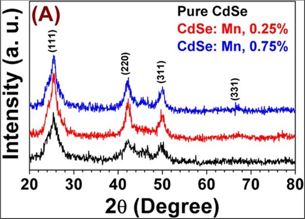
Download figure
where D is the crystallite size, βhkl is the full - width at half - maximum (FWHM) of the diffraction peak measured in radian, λ (1.54 Å) is the wavelength of X-ray CuKα1 radiation, and θ is the angle of diffraction.
Lattice constant of all cubic CdSe NC samples were calculated by using formula 27, 28:

where, 𝑎 is lattice constant, h, k, l are Miller indices and d is the interplanar spacing which was calculated using Bragg’s formula:

where, θ is the angle between the incident beam and the reflection lattice planes, n = 1 for first order. Corresponding to the planes (111), (220), (311) and (331), the calculated values of d- spacing, lattice constant 𝑎 and crystallite size for cubic phase 0%, 0.25% and 0.75% Mn2+ doped CdSe NCs are given in Table 1
Table 1. Structural parameters for 0%, 0.25%, and 0.75% Mn2+doped CdSe NCs.| (hkl) | Standard JCPDS data for CdSe sample | Data for synthesized CdSe : Mn Samples | ||||||||||
| 2 θ (⁰) | d (Å) | a (Å) | 2 θ (⁰) | d (Å) | a (Å) | 0% Mn | 0.25% Mn | 0.75% Mn | ||||
| FWHM (radian) | D (nm) | FWHM (radian) | D (nm) | FWHM (radian) | D (nm) | |||||||
| (111) | 25.375 | 3.51 | 6.0795 | 25.36 | 3.5079 | 6.0759 | 0.049956 | 2.84 | 0.042421 | 3.35 | 0.043469 | 3.27 |
| (220) | 42.044 | 2.149 | 6.0783 | 42.28 | 2.1350 | 6.0388 | 0.053294 | 2.79 | 0.023797 | 6.24 | 0.025356 | 5.86 |
| (311) | 49.741 | 1.833 | 6.0794 | 49.60 | 1.8357 | 6.0885 | 0.038204 | 3.99 | 0.029801 | 5.12 | 0.024902 | 6.13 |
| (331) | 67.142 | 1.3941 | 6.0767 | 67.18 | 1.3918 | 6.0666 | --- | --- | --- | --- | --- | --- |
| Average value of crystallite size D (nm) | 3.21 | 4.91 | 5.09 | |||||||||
Furthermore, with powder, the peak broadening is due to a linear combination of the contribution from nanocrystalline nature and local strain in the crystal structure from defects 29, 30. The strain ε induced in powders due to crystal imperfection and distortion can be calculated using the formula:
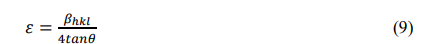
The strain ε and crystallite size D of the Mn2+ doped CdSe NCs were estimated by Williamson – Hall (W – H) method 30. The observed FWHM of diffraction peaks is simply the sum of the Eqs.(6) & (9) which results in the Williamson – Hall Eq. (10).
In Figure 1(B) the values of 𝛽hkl𝑐𝑜𝑠𝜃 on y-axis were plotted as a function of 4sin𝜃 on x-axis. From the linear fit of data, the crystallite size D was estimated from the y-intercept, and the strain ε, from the slope of the linear fit. In this study, the crystallite size D obtained at zero strain were about 3.21, 4.91 and 5.09 nm with different Mn2+ concentrations (0 – 0.75%), respectively. These crystallite sizes are smaller than the exciton Bohr radius of CdSe 𝛼B~5.6𝑛𝑚 31 and increase as the concentration of Mn2+ ions increases in CdSe NCs. The result indicates that the quantum-size effect appears in all the samples. The strain values ε were found to be -0.01538, -0.02417 and - 0.01538 for 0%, 0.25% and 0.75% Mn2+ doped CdSe NCs, respectively. The negative sign means that the Mn2+CdSe NCs have a compressive strain in all the samples 29. The appearance of the compressive strain is due to the substitution of Cd2+ (0.92 Å) ions with Mn2+ (0.67 Å) ions of the smaller radius in the CdSe host. In CdSe host the Mn-Se bond length (2.364 Å) is slightly smaller than the Cd-Se bond length (2.597Å) which leads to a lattice disorder and the formation of strain in the CdSe lattice 32.
Figure 1. (B) W-H plots of CdSe: Mn (0%, 0.25% and 0.75%) NCs
Download figure
TEM analysis
Figure 2 shows transmission electron microscopy (TEM) images, high-resolution transmission electron microscopy (HRTEM) micrographs and selected area electron diffraction (SAED) patterns of 0%, 0.25% and 0.75% Mn2+ doped CdSe NCs. HRTEM was used for structural and morphological analysis of undoped and Mn2+ doped CdSe NCs. TEM images of undoped and Mn2+ doped CdSe NCs are shown in Figure 2(A, B &C) which indicates that the average size of undoped and doped CdSe NCs lies between 5 - 15 nm and increases with increase in doping concentration of Mn2+ ions in CdSe NCs. The difference between XRD and TEM data may be due to:
(i) there may be more than one crystallite in single grain;
(ii)there may be some agglomeration of the particles 33.
Figure 2. TEM images (A-C), HRTEM micrographs (D-F) and SAED patterns (G-I) of 0%, 0.25%,and 0.75% Mn2+ doped CdSe NCs, respectively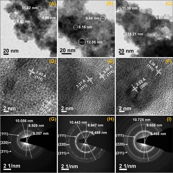
Download figure
HRTEM micrographs of undoped and Mn2+ doped CdSe NCs are given in Figure 2(D, E & F) which shows that particles are well defined. The lattice fringes visible in the HRTEM micrographs of a single CdSe NC are indicative of the crystalline nature of the particles. The lattice spacing ~3.5 Å corresponds to (111) planes and ~2.1 Å corresponds to (220) planes of cubic CdSe 34.
Figure 2(G, H & I) shows broad diffuse SAED patterns of undoped and Mn2+ doped CdSe NCs. These patterns show a system of spots which form concentric rings corresponding to diffraction from various atomic planes. Each spot corresponds to reflection from a single – crystal particle of specific orientation. The presence of single crystals of various orientations leads to the formation of rings of spots 35. SAED pattern shows principally three rings ascribed to Miller indices (111), (220) and (311), respectively of the cubic CdSe phase. This indicates that as the concentration of Mn2+ ions increases, crystallinity of the sample slightly changes. Table 2 shows the values d- spacing for 0%, 0.25%, and 0.75% Mn2+ doped CdSe NCs corresponding to Miller indices (111), (220) and (311), respectively obtained from SAED pattern which are in good agreement with the cubic structure of CdSe (JCPDS card No. 19-0191).
SEM and elemental analysis:
Scanning electron microscopy (SEM) is a versatile technique to study morphology of nanomaterialsFigure 3(A, B & C) shows the FEG-SEM photographs of 0% (undoped), 0.25% and 0.75% Mn2+ doped CdSe NCs. The average diameter (crystallite size) of almost spherical undoped and doped CdSe NCs lies between 5 nm to 20 nm and increases with increase in doping concentration of Mn2+ ions in CdSe NCs 36, which is in good agreement with HRTEM result discussed above.
Table 2. Interplanar spacing d for 0%, 0.25%, and 0.75% Mn2+ doped CdSe NCs| ( hkl ) | Interplaner spacing d (Å) | ||
| Undoped CdSe | CdSe : Mn, 0.25% | CdSe : Mn, 0.75% | |
| (111) | 3.8044 | 3.6456 | 3.6576 |
| (200) | 2.3504 | 2.2354 | 2.2084 |
| (220) | 1.9889 | 1.9152 | 1.8648 |
Figure 3. SEM photographs (A-C) and EDS spectra (D-F) of 0%, 0.25%, and 0.75% Mn2+ doped CdSe NCs, respectively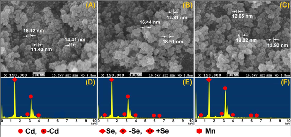
Download figure
The Energy Dispersive Spectrometer (EDS) analysis can be used to determine the composition of a specimen as a whole as well as the composition of individual componentsFigure 3 (D, E & F) shows the EDS spectra of 0%, 0.25% and 0.75% Mn2+ doped CdSe NCs, respectively, which confirm the presence of the Cd, Se and Mn elements. The data reveal the formation of undoped and Mn2+ doped CdSe with appropriate ratio of Cd : Se : Mn in the prepared NCs. The elemental composition of the synthesized 0%, 0.25%, and 0.75% Mn2+ doped CdSe NCs are given in Table 3 It is very important to note that no additional peaks corresponding to impurities or contaminants are observed, which confirms the purity of the NCs prepared 37, 38.
Table 3. EDS elemental Cd:Se:Mn weight % and atomic % of 0%, 0.25%, and 0.75% Mn2+ doped CdSe NCs| Element | Undoped CdSe | CdSe : Mn, 0.25% | CdSe : Mn, 0.75% | |||
| Weight% | Atomic% | Weight% | Atomic% | Weight% | Atomic% | |
| SeL | 9.78 | 34.05 | 8.12 | 17.24 | 8.37 | 35.27 |
| Mn K | 0.00 | 0.00 | 1.06 | 8.86 | 5.48 | 18.23 |
| Cd L | 90.22 | 65.95 | 90.82 | 73.90 | 86.15 | 46.50 |
| Total | 100 | 100 | 100 | |||
|---|---|---|---|---|---|---|
UV/Vis Analysis
The UV/V is absorption spectra for both undoped and Mn2+ doped CdSe NCs are shown in Figure 4(A). Direct optical band gap energies were obtained as 2.54 eV, 2.27 eV and 2.24 eV for 0%, 0.25% and 0.75% Mn2+ doped CdSe NCs with the help of Tauc plot as shown in Figure 4(B) using the classical relationship of near edge optical absorption of semiconductors 39, 40:
where A is a constant, Eg is the energy band gap of the materials, h is the Planck’s constant, ν is the frequency and exponent n depends on the type of transition. For direct allowed transition n = 1/2, for indirect allowed transition n = 2, for direct forbidden transition n = 3/2 and for forbidden indirect transition n = 3 41. To determine the possible transitions, (αhν)2 vs. hν curves are plotted and corresponding band gap energies are obtained from extrapolating the straight line of the curves for zero absorption coefficient on hν axis. The optical band gap energy decreases from 2.54 eV to 2.24 eV as the concentration of Mn2+ ions increases from 0% to 0.75% in CdSe NCs. This small change in band gap energy may be due to direct transfer of energy between semiconductor – excited states and 3d state of Mn2+ ions 40, 41.
The UV/V is absorption spectra for both undoped and Mn2+doped CdSe NCs show blue shift of ~0.6 eV as compared to the absorption edge (1.74 eV) for bulk CdSe at 300 K 29 as shown in Figure 4(A). The shift to shorter wavelength in absorption peak was obviously caused by quantum confinement effect due to decrease in particle size.
Figure 4. (A) UV – Visible absorption spectra for undoped and Mn2+ doped CdSe NCs and (B) Tauc plot of (αhν)2 versus hν for undoped and Mn2+ doped CdSe NCs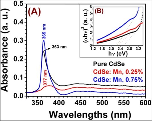
Download figure
Furthermore, for strong confinement, in which NC diameter D is smaller than the exciton Bohr radius
 for bulk CdSe), the quantized energy levels of electrons and holes can be found from the solution of Schrödinger equation of Hamiltonian in Eq. (13) for a particle in a spherical box 42
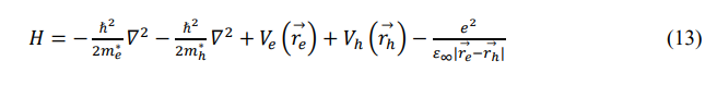
where the first two terms are the kinetic energy of an electron and a hole, the third and fourth terms represent the confinement potential energies and finally, the last term represents the Coulomb electron-hole interaction. The Eigen values of Hamiltonian in Eq. (13) yield the following expression for band gap energy of NC (the 1s - 1s excited state energy) 42:
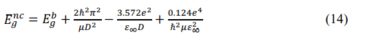
where Encg and Ebg are the band gap energies for CdSe NCs and bulk CdSe semiconductor, respectively h=h/2π with h representing Planck’s constant, D is the diameter of the NCs, 𝜀∞ is the optical dilectric constant of the bulk CdSe semiconductor and µ is the reduced mass of the exciton given as µ=
 is the electron mass at rest in vacuum 𝜀∞=8.5𝜀𝑜43). Second and third terms represent the quantum confinement and the Coulomb interaction, respectively. Finally, last term represents the Rydberg correlation energy (polarisation term). The diameter of the NC can be calculated by converting Eq. (14) into a quadratic equation for the D as unknown:𝐴𝐷2+𝐵𝐷+𝐶=0, where A, B and C are material dependent parameters. From the calculated band gap energies as described above and by using Eq. (14) (neglecting polarization term), the average size of 0%, 0.25% and 0.75% and Mn2+ doped CdSe NCs has been calculated as 1.69 nm, 1.77 nm and 1.78 nm. The calculated values of average size of CdSe NCs from optical absorption study also increase with increase in doping concentration of Mn2+ ions and matches well with those obtained from XRD data described above Table 1.
PL analysis
Figure 5 presents PL spectra of undoped and Mn2+ doped CdSe NCs with excitation wavelength 360 nm at room temperature. The PL spectra show distinctive dual colour emissions. The narrow band emission centered at 380 nm with FWHM ~11 nm is assigned to the CdSe host and the broad emission nearly at 460 nm with FWHM ~49 nm is assigned to Mn2+ ions doped in the CdSe NCs, which can be attributed to a transition between 4T1 and 6A1 energy levels of the Mn2+ 3d states 44. The intense Mn2+ luminescence indicates that the doped Mn2+ ions could serve as an efficient acceptor of the energy from the excited CdSe host 45. The PL spectrum sufficiently confirms the existence of Mn2+ ions in the synthesized CdSe NCs. The luminescence intensity and FWHM of CdSe NCs change with the change in concentration of Mn2+ ions 46. 0.25 % Mn2+ doped CdSe NCs show maximum luminescence intensity while 0.75 % Mn2+ doped CdSe NCs show less luminescence intensity but greater than undoped CdSe NCs. This means that for larger concentration of Mn2+ ions the luminescence intensity becomes smaller. In highly doped sample (CdSe: Mn, 0.75 %) Mn ions are placed near the surface of the core and that the Mn – Mn pair formation is a possible reason for the reduction of intensity of luminescence. The magnetization of Mn reduces due to antiferromagnetic coupling of Mn spins and therefore luminescence intensity reduces. In lightly doped sample (CdSe: Mn, 0.25 %) the Mn related splitting energy decreases thereby relatively high luminescence intensity is observed 47.
Figure 5. PL spectra of 0%, 0.25%, and 0.75% Mn2+ doped CdSe NCs at room temperature.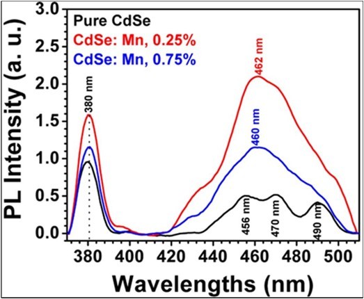
Download figure
EPR analysis
0.25% and 0.75% Mn2+ doped CdSe NCs show well-resolved X-band EPR spectra Figure 6, at room temperature. Between the six major peaks that arise from the electron-nuclear hyperfine interaction at the Mn2+ (S=5/2, I=5/2, L=0), several smaller features are observed that contain information about the zero-field splitting of the Mn2+6A1 ground state 8, 48. The spectrum can be explained by the following spin Hamiltonian:

where 𝜇B is the Bohr magneton, B is the applied magnetic field, S and I are the electron and nuclear spin
operators 8. The first term gives the Zeeman interaction with isotropicg. The second term is the zero-field splitting term and the third term is the cubic-field splitting. The fourth term represents the hyperfine interaction with the 55Mn nucleus. In strong applied magnetic field for Mn, the first term (𝜇B 𝑩⋅𝒈⋅𝑺)≫𝑎. Therefore, the third term is neglected in Eq. (15) 49, 50. The above hyperfine features are reproduced in spectral simulations (Figure 6, bottom) using the same spin Hamiltonian (Eq. 15) and spectroscopic splitting factor 𝑔, hyperfine parameter A and second- rank axial zero-field splitting D parameters deduced from EPR study of Mn2+ doped CdSe NCs. This demonstrates Mn2+ substitution at the axial cation site of the cubic CdSe lattice in these NCs. For Mn2+ there are only six allowed transitions corresponding to ΔMs = ±1 and ΔMI = 0. In CdSe lattice containing substitutional Mn2+, hyperfine lines are possible due to ±5/2↔±3/2, ±3/2↔±1/2 and +1/2↔-1/2 transitions. But the anisotropic contributions from ±5/2↔±3/2 and ±3/2↔±1/2 transitions are cancelled due to random orientations. Thus only +1/2↔-1/2 transition gives six lines spectrum 10.
The Mn2+ doped CdSe NCs contain various types of disorders and differences in surface passivation of each crystal. The EPR detects average of all the above properties. The values of 𝑔, A and D parameters for Mn2+ doped CdSe NCs obtained from EPR spectra are given in Table 4.The 𝑔 values show that the doping of Mn2+ ions in CdSe NCs is present. The values of A for Mn2+ doped CdSe NCs are presenting the characteristics of Mn2+ ions in an octahedral crystal field. The smaller values of D for Mn2+ doped CdSe NCs show little distortion. In EPR
Figure 6. Experimental and Simulated EPR spectra of (A) 0.25% Mn2+ doped CdSe NCs and (B) 0.75% Mn2+ doped CdSe NCs at room temperature (Frequency = 9.45 GHz)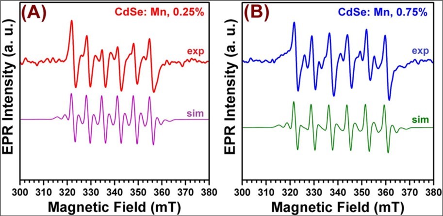
Download figure
| Samples | g | A (10 -4 cm -1 ) | D (10 -4 cm -1 ) |
| CdSe : Mn, 0.25% | 1.991 | 61.70 | 31.69 |
|---|---|---|---|
| CdSe : Mn, 0.75% | 1.978 | 70.05 | 33.36 |
spectra all the samples provide sextet splitting. The peak-to-peak line widths of EPR lines are about 66 G for 0.25% Mn2+ and 76 G for 0.75% Mn2+ from which we conclude that the Mn2+ ions are incorporated within the CdSe and not on the surface of CdSe NCs 10. As Mn concentration is increased, Mn – Mn interaction increases due to which the intensity, line width and distortion of EPR spectra slightly increase 39.
Conclusions
The synthesis of Mn2+ doped CdSe NCs by the chemical route without using any external capping agent and their structural and optical characterization have been reported. The NC size was confirmed by XRD, HRTEM. SEM and UV/Vis analysis. Spectroscopic results shows that the absorption peaks are blue shifted from the absorption edge of the bulk. The band gaps of all the samples are found to increase as compared to bulk CdSe which may be attributed to quantum confinement. EDS, PL and EPR spectra confirm the doping of Mn2+ ions in CdSe NCs. The PL spectra show distinctive dual colour emissions nearly at 380 nm and 465 nm for CdSe host and Mn2+ ions doped in CdSe NCs. From EPR study it is seen that the values of the hyperfine parameter A, the second-order axial zero-field splitting parameter D and the electron spectroscopic splitting factor gdecrease as Mn2+ concentration increases in CdSe NCs. On the basis of results the materials studied here are better candidate of optoelectronic devices. like emitter for colour display, optical fiber amplifier, chemical sensor and low threshold laser.
References
- 1.Dai Q, E M Sabio, Wang W, Tang J. (2014) Pulsed laser deposition of Mn doped CdSe quantum dots for improved solar cell performance. , Appl. Phys. Lett 104, 183901-183906.
- 2.Beaulac R, Schneider L, P I Archer, Bacher G, D R Gamelin. (2009) Light-Induced Spontaneous Magnetization in Doped Colloidal Quantum Dots. , Science 325, 973-976.
- 3.B, X W Wang, J L Cui, L H, Cao Y et al. (2016) Synthesis of Mn-doped zinc blende CdSe nanocrystals for quantum dot-sensitized solar cells. , Res. Chem. Intermed 42, 6255-6263.
- 4.Beaulac R, P I Archer, S T Ochsenbein, D R Gamelin. (2008) Mn2+-Doped CdSe Quantum Dots: New Inorganic Materials for Spin-Electronics and Spin-Photonics. , Adv. Funct. Mater 18, 3873-3891.
- 5.V A, Janssen N, J V Rijssel, Beaulac R, D R Gamelin. (2010) Tunable Dual Emission in Doped Semiconductor Nanocrystals, Nano Lett. 10, 3670-3674.
- 6.Beaulac R, P I Archer, Liu X, Lee S, G M Salley et al. (2008) . Spin-Polarizable Excitonic Luminescence in Colloidal Mn2+-Doped CdSe Quantum Dots, Nano Lett 8, 1197-1201.
- 7.Kripal R, Bajpai M. (2010) . , EPR and Optical Absorption Studies of Mn2+Doped Diglycine Calcium Chloride Tetrahydrate, Chi. J. Phys 48, 671-682.
- 8.Zheng W, Wang Z, Wright J, Goundie B, N S Dalal et al. (2011) Probing the Local Site Environments in Mn:CdSe Quantum Dots. , J. Phys. Chem. C 115 23305-23314.
- 9.Kripal R, A K Shukla. (2006) . EPR Studies of Mn2+-Doped Diammonium Hexaaqua Magnesium (II) Sulfate, Z. Naturforsch. 61a 683-687.
- 10.Kripal R, U M Tripathi. (2017) Synthesis and Characterization of Mn2+Doped Cadmium Sulfide Quantum Dots. , Adv. Sci. Eng. Med 9, 130-136.
- 11.N A Khan, Humayun M, Usman M, Z A Ghazi, Naeem A et al. (2021) Structural Characteristicsand Environmental Applications ofCovalent Organic Frameworks.Energies,14. 2267-2288.
- 12.Humayun M, Ullah H, Cao J, Pi W, Yuan Y et al. (2020) . Experimental and DFT Studies of Au Deposition Over WO3/g-C3N4 Z-Scheme Heterojunction, Nano-Micro Lett 12, 7-25.
- 13.Raziq F, Humayun M, Ali A, Wang T, Khan A et al.. Synthesis of S-Doped Porous g-C3N4 by Using Ionic Liquids and Subsequently Coupled with Au-TiO2 for Exceptional Cocatalyst-Free Visible-Light Catalytic Activities,AppliedCatalysisB:Environmental(2018) , https://doi.org/10.1016/j.apcatb.2018.06.009 .
- 14.Noureen L, Xie Z, Hussain M, Li M, Lyu Q et al. (2021) BiVO4 and reduced graphene oxide composite hydrogels for solar-driven steam generation and decontamination of polluted water. , Solar Energy Materials & Solar Cells 222, 110952-110958.
- 15.Pi W, Humayun Y Li M, Yuan Y, Cao J, Ali S et al.Properly aligned band structures in B-TiO2/MIL53(Fe)/g-C3N4 ternary nanocomposite can drastically improve its photocatalytic activity for H2 evolution: Investigations based on the experimental results. , International Journal of Hydrogen Energy 10.
- 16.Humayun M, Pi W, Yuan Y, Shu L, Cao J et al. (2021) A rational design of g-C3N4-based ternary composite for highly efficient H2 generation and 2,4-DCP degradation. , J. Colloid and Interface Science 599, 484-496.
- 17.Haleem A, Shafiq A, S Q Chen, Nazar M. (2023) A Comprehensive Review on Adsorption. Photocatalytic and Chemical Degradation of Dyes and Nitro-Compounds over Different Kinds of Porous and Composite Materials, Molecules 28, 1081-1119.
- 18.L A Shah, Malik T, Siddiq M, Haleem A, Sayed M et al. (2019) TiO2 nanotubes doped poly(vinylidene fluoride) polymer membranes (PVDF/TNT) for efficient photocatalytic degradation of brilliant green dye. , J. Environmental Chemical Engineering 10-1016.
- 19.Bibi S, Ahmad A, Anjum M A R, Haleem A, Siddiq M et al. (2021) Photocatalytic degradation of malachite green and methylene blue over reduced graphene oxide (rGO) based metal oxides (rGO-Fe3O4/TiO2) nanocomposite under UV-visible light irradiation. , J. Environmental Chemical Engineering 9, 105580-105591.
- 20.A S Khan, Muhammad S, Ambreen J, Farooq M, Ihsan J et al.Fabrication of Manganese Oxide-silica Based Functional Polymer Composite Membranes and Their Environmental Application, Polymer-Plastics Technology and Materials. , DOI: 10-1080.
- 21.Haleem S Q Chen A, Ullah M Siddiq M, W D He. (2021) Highly porous cryogels loaded with bimetallic nanoparticles as an efficient antimicrobial agent and catalyst for rapid reduction of water-soluble organic contaminants. , J. Environmental Chemical Engineering 9(6), 106510.
- 22.Wang X, Xi G, Liu Y, Qian Y. (2008) . Controllable Synthesis of PbSe Nanostructures and Growth Mechanisms, Cryst. Growth Des 8, 1406-1411.
- 23.Kumar P, Singh K. (2008) Element Directed Aqueous Solution Synthesis of Copper Telluride Nanoparticles, Characterization, and Optical Properties, Cryst. Growth Des. 9, 3089-3094.
- 24.Zhong X, Han M, Dong Z, T J White, Knoll W. (2003) Composition-Tunable ZnxCd1-xSe Nanocrystals with High Luminescence and Stability. , J. Am. Chem. Soc 125, 8589-8594.
- 25.Wanga Y, Lianga X, Maa X, Hua Y, Hub X et al. (2014) Simple and greener synthesis of highly photoluminescence Mn2+-doped ZnS quantum dots and its surface passivation mechanism. , Appl. Surf. Sci 316, 54-61.
- 26.Ma C, Zhou M, Wu D, Feng M, Liu X et al. (2015) One-step hydrothermal synthesis of cobalt and potassium codopedCdSe quantum dots with high visible light photocatalytic activity. , Cryst. Eng. Comm 17, 1701-1709.
- 27.Bansal P, Jaggi N, S K Rohilla. (2012) Green” Synthesis of CdS nanoparticles and effect of capping agent concentration on crystallite size. , Res. J. Chem. Sci 2, 69-71.
- 28.S R, S L Rayar, Selvarajan P. (2015) Effect of annealing and dopants on the physical properties of CdS nanoparticles. , Intl. J. Adv. Sci. Tech. Res 5, 198-207.
- 29.Bindu P, Thomas S. (2014) Estimation of lattice strain in ZnO nanoparticles: X-ray peak profile analysis. , J. Theor. Appl. Phys 8, 123-134.
- 30.M N Boraha, B J, Chalihab S, D P Gogoib, McFarlanea U et al. (2013) Structural analysis of chemically deposited nanocrystalline CdSe films. , J.Exp. Nanosci 8, 273-279.
- 31.R W Meulenberg, Lee J R I, Wolcott A, J Z Zhang, L J Terminello et al. (2009) Determination of the Exciton Binding Energy in CdSe Quantum Dots. , ACS Nano 3, 325-330.
- 32.Xu S, Xu X, Wang C, Zhao Z, Wang Z et al. (2016) Theoretical and experimental investigation of doping M in ZnSe (M Mn, Ag, Cu) clusters: optical and bonding characteristics. , Luminescence 31, 312-316.
- 33.Kripal R, A K Gupta. (2010) EPR and optical studies of ZnS: Mn nanoparticles. , Chalcogenide Lett 7, 203-209.
- 34.W C Kwak, Y M Sung, T G Kim, W S Chae. (2007) Synthesis of Mn-doped zinc blende CdSe nanocrystals. , Appl. Phys. Lett 90, 173111-173112.
- 35.Yue S, Zhou Y, Zou S, Wang L, Liu H et al. (2017) Chemically Tunable, All-Inorganic- Based White-Light Emitting 0D–1D Heterostructures. , Adv. Optical Mater 5, 1700089-1700107.
- 36.Zhang C, Liu S, Liu X, Deng F, Xiong Y et al. (2018) Incorporation of Mn2+into CdSe quantum dots by chemical bath co-deposition method for photovoltaic enhancement of quantum dot-sensitized solar cells, .R. Soc. open sci. 5. 171712-171720.
- 37.Singh S, A K Shrivastava, Tapdiya S. (2017) Synthesis and characterization of Mn composition effect on CdSe thin films. , Adv. Mater. Proce 2, 367-370.
- 38.D A Reddy, Liu C, R P Vijayalakshmi, B K Reddy. (2014) Effect of Al doping on the structural, optical and photoluminescence properties of ZnS nanoparticles. , J. Alloys Compd 582, 257-264.
- 39.Halder G, Bhattacharya S. (2015) Plight of Mn Doping in Colloidal CdS Quantum Dots to Boost the Efficiency of Solar Cells. , J. Phys. Chem. C 119, 13404-13412.
- 42.H S Pisheh, Gheshlaghi N, Unlu H. (2017) Composition tuning of bandgap and diameter of CdSe/Cd1-xZnxS core/shell quantum dots. , Mater. Sci. Semicond. Process 68, 295-301.
- 43.Adachi S. (2005) . Properties of Group IV, III-V Semiconductors, Wiley Series in Materials for Electronic and Optoelectronic Applications , John Willey .
- 44.H Y Chen, Maiti S, D H Son. (2012) Doping Location-Dependent Energy Transfer Dynamics in Mn-Doped CdS/ZnS Nanocrystals. , ACS Nano 6, 583-591.
- 45.Pradhan N. (2016) Red-Tuned Mn d-d Emission in Doped Semiconductor Nanocrystals. , Chem. Phys. Chem 17, 1087-1094.
- 46.Manikandan A. (2018) Influence of Mn2+ions on both core/shell of CuInS2/ZnS nanocrystals. , Mater. Res. Bull 98, 265-274.
- 47.Taguchi S, Ishizumi A, Tayagaki T, Kanemitsu Y. (2009) Mn–Mn couplings in Mn-doped CdS nanocrystals studied by magnetic circular dichroism spectroscopy. , Appl. Phys. Lett 94, 173101-173103.
- 48.Bhattacharyya S, Zitoun D, Gedanken A. (2008) One-Pot Synthesis and Characterization of Mn2+-Doped Wurtzite CdSe Nanocrystals Encapsulated with Carbon. , J. Phys. Chem. C 112, 7624-7630.